In Part Two of this series, we indicated that a key element in a successful static control program was the identification of those items (components, assemblies, and finished products) that are sensitive to ESD and the level of their sensitivity. Damage to an ESDS device by the ESD event is determined by the device’s ability to dissipate the energy of the discharge or withstand the current levels involved. This is known as device “ESD sensitivity” or “ESD susceptibility”.
Some devices may be more readily damaged by discharges occurring within automated equipment, while others may be more prone to damage from handling by personnel. In this article we will cover the models and test procedures used to characterize, determine, and classify the sensitivity of components to ESD. These test procedures are based on the two primary models of ESD events: Human Body Model (HBM) and Charged Device Model (CDM). The models used to perform component testing cannot replicate the full spectrum of all possible ESD events. Nevertheless, these models have been proven to be successful in reproducing over 99% of all ESD field failure signatures. With the use of standardized test procedures, the industry can
- Develop and measure suitable on-chip protection.
- Enable comparisons to be made between devices.
- Provide a system of ESD sensitivity classification to assist in the ESD design and monitoring requirements of the manufacturing and assembly environments.
- Have documented test procedures to ensure reliable and repeatable results.
Human Body Model (HBM) Testing
One of the most common causes of electrostatic damage is the direct transfer of electrostatic charge through a significant series resistor from the human body or from a charged material to the electrostatic discharge sensitive (ESDS) device. When one walks across a floor, an electrostatic charge accumulates on the body. Simple contact of a finger to the leads of an ESDS device or assembly allows the body to discharge, possibly causing device damage. The model used to simulate this event is the Human Body Model (HBM).

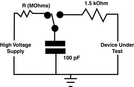
Figure 1: Typical Human Body Model Circuit
The Human Body Model is the oldest and most commonly used model for classifying device sensitivity to ESD. The HBM testing model represents the discharge from the fingertip of a standing individual delivered to the device. It is modeled by a 100 pF capacitor discharged through a switching component and a 1.5kW series resistor into the component. This model, which dates from the nineteenth century, was developed for investigating explosions of gas mixtures in mines. It was adopted by the military in MIL-STD-883 Method 3015, and is referenced in ANSI/ESDA-JEDEC JS-001-2010: Electrostatic Discharge Sensitivity Testing — Human Body Model. This document replaces the previous ESDA and JEDEC methods, STM5.1-2007 and JESD22-A114F respectively. A typical Human Body Model circuit is presented in Figure 1.
Testing for HBM sensitivity is typically performed using automated test systems. The device is placed in the test system and contacted through a relay matrix. ESD zaps are applied. A part is determined to have failed if it does not meet the datasheet parameters using parametric and functional testing.
Charged Device Model (CDM) Testing
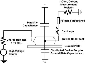
Figure 3: Typical Charged Device Model Test
The transfer of charge from an ESDS device is also an ESD event. A device may become charged, for example, from sliding down the feeder in an automated assembler. If it then contacts the insertion head or another conductive surface, which is at a lower potential, a rapid discharge may occur from the device to the metal object. This event is known as the Charged Device Model (CDM) event and can be more destructive than the HBM for some devices. Although the duration of the discharge is very short–often less than one nanosecond–the peak current can reach several tens of amperes.
The device testing standard for CDM (ESD STM5.3.1: Electrostatic Discharge Sensitivity Testing – Charged Device Model) was originally published in 1999. The test procedure involves placing the device on a field plate with its leads pointing up, then charging it and discharging the device. Figure 3 illustrates a typical CDM test circuit. The CDM 5.3.1 ESDA document was last published in 2009.
Other Test Methods
Machine Model (MM) Testing
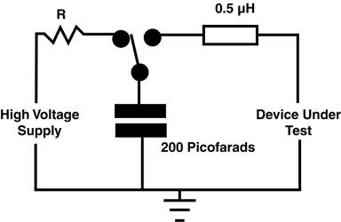
Figure 2: Typical Machine Model Circuit
A discharge which is different in shape and size to the HBM event also can occur from a charged conductive object, such as a metallic tool, or an automatic equipment or fixture. Originating in Japan as the result of trying to create a worst-case HBM event, the model is known as the Machine Model. This ESD model consists of a 200 pF capacitor discharged directly into a component with no series DC resistor in the output circuitry. The industry is in the process of removing this model from qualification requirements. The technical background on this change is described in Industry Council White Paper 1, “A Case for Lowering Component Level HBM/MM ESD Specifications and Requirements.”
As a worst-case human body model, the Machine Model may be over severe. However, there are real-world situations that this model may simulate, for example the rapid discharge from the metallic contacts on a charged board assembly or from the charged cables or handles/arms of an automatic tester.
Testing of devices for MM sensitivity using ESD Association standard ESD STM5.2: Electrostatic Discharge Sensitivity Testing — Machine Model is similar in procedure to HBM testing. The test equipment is the same, but the test head is slightly different. The MM version does not have a 1,500 ohm resistor, but otherwise the test board and the socket are the same as for HBM testing. The series inductance, as shown in Figure 2, is the dominating parasitic element that shapes the oscillating machine model wave form. The series inductance is indirectly defined through the specification of various waveform parameters like peak currents, rise times and the period of the waveform. The MM 5.2 document was last published in 2009.
Socketed Device Model (SDM) Testing
SDM testing is similar to testing for HBM and MM sensitivity. The device is placed in a socket, charged from a high-voltage source and then discharged. This model was originally intended to provide an efficient way to do CDM testing. However, the model did not have sufficient correlation with the CDM standard and there was too great a dependency on the specific design of the SDM tester. A Standard Practice (SP) document (SP), SDM-5.3.2, was first published in 2002, and re-published in 2008. A technical report, ESD TR5.3.2 (formerly TR08-00) : Socket Device Model (SDM) Tester is also available from the ESD Association.
Device Sensitivity Classification
The HBM and CDM methods include a classification system for defining the component sensitivity to the specified model (See Tables 1 and 2). These classification systems have a number of advantages. They allow easy grouping and comparing of components according to their ESD sensitivity and the classification gives you an indication of the level of ESD protection that is required for the component.
| Table 1 ESDS Component Sensitivity Classification – Human Body Model (Per ESD STM5.1-2007) |
|
|---|---|
| Class | Voltage Range |
| Class 0 | <250 volts |
| Class 1A | 250 volts to <500 volts |
| Class 1B | 500 volts to < 1,000 volts |
| Class 1C | 1000 volts to < 2,000 volts |
| Class 2 | 2000 volts to < 4,000 volts |
| Class 3A | 4000 volts to < 8000 volts |
| Class 3B | ≥ 8000 volts |
| Table 2 ESDS Component Sensitivity Classification – Charged Device Model (Per ESD STM5.3.1-2009) |
|
|---|---|
| Class | Voltage Range |
| Class C1 | <125 volts |
| Class C2 | 125 volts to <250 volts |
| Class C3 | 250 volts to <500 volts |
| Class C4 | 500 volts to <1,000 volts |
| Class C5 | 1,000 volts to <1,500 volts |
| Class C6 | 1,500 volts to <2,000 volts |
| Class C7 | ≥ 2,000 volts |
A fully characterized component should be classified using Human Body Model, and Charged Device Model. For example, a fully characterized component may have 2 of the following: Class 1B (500 volts to <1000 volts HBM) and Class C3 (500 volts to <1000 volts CDM). This would alert a potential user of the component to the need for a controlled environment, whether assembly and manufacturing operations are performed by human beings or machines.
A word of caution; however, these classification systems and component sensitivity test results function as guides, not necessarily as absolutes. The events defined by the test data produce narrowly restrictive data that must be carefully considered and judiciously used. The two ESD models represent discrete points used in an attempt to characterize ESD vulnerability. The data points are informative and useful, but to arbitrarily extrapolate the data into a real world scenario can be misleading. The true utility of the data is in comparing one device with another and to provide a starting point for developing your ESD control programs.
Summary
Device failure models and device test methods define the sensitivity of the electronic devices and assemblies to be protected from the effects of ESD. With this key information, you can design more effective ESD control programs.
For Further Reference
- ESD STM5.1-2007: Electrostatic Discharge Sensitivity Testing — Human Body Model, ESD Association, Rome, NY.
- ESD STM5.2-2009: Electrostatic Discharge Sensitivity Testing — Machine Model, ESD Association, Rome, NY.
- ESD STM5.3.1-2009: Electrostatic Discharge Sensitivity Testing — Charged Device Model, ESD Association, Rome, NY.
- ESD TR 5.3.2- (formerly TR08-00): Socket Device Model (SDM) Tester, ESD Association, Rome, NY.
- ESD Industry Council White Paper 1: “A Case for Lowering Component Level HBM/MM ESD Specifications and Requirements,” August 2008.
- ESD Industry Council White Paper 2: “A Case for Lowering Component Level CDM ESD Specifications and Requirements,” March 2009.
- “A Closer Look at the Human ESD Event,” Hyatt, Hugh, et al, EOS/ESD Symposium Proceedings, 1981, ESD Association, Rome, NY.
- “Charged Device Model Testing: Trying to Duplicate Reality,” Avery, L.R., EOS/ESD Symposium Proceedings, 1987, ESD Association, Rome, NY.
- “Critical Issues Regarding ESD Sensitivity Classification Testing,” Pierce, Donald C., EOS/ESD Symposium Proceedings,1987, ESD Association, Rome, NY.
- “Beyond MIL HBM Testing – How to Evaluate the Real Capability of Protection Structures, Avery, L.R., EOS/ESD Symposium Proceedings, 1991, ESD Association, Rome, NY.
- “Mechanisms of Charged-Device Electrostatic Discharges,” Renninger, Robert G., EOS/ESD Symposium Proceedings, 1991, ESD Association, Rome, NY.
- “Analysis of HBM ESD Testers and Specifications Using a 4th Order Lumped Element Model,” Verhaege, Koen, et al, EOS/ESD Symposium Proceedings, 1993, ESD Association, Rome, NY.
- “A Comparison of Electrostatic Discharge Models and Failure Signatures for CMOS Integrated Circuit Devices,” Kelly, M., et al, EOS/ESD Symposium Proceedings, 1995, ESD Association, Rome, NY.
- “Study of ESD Evaluation Methods for Charged Device Model,” Wada, Tetsuaki, EOS/ESD Symposium Proceedings, 1995, ESD Association, Rome, NY.
- “A Compact Model for the Grounded-Gate nMOS Behavior Under CDM ESD Stress,” Russ, Christian, et al, EOS/ESD Symposium Proceedings, 1996, ESD Association, Rome, NY.
- “Recommendations to Further Improvements of HBM ESD Component Level Test Specifications,” Verhaege, Koen, et al, EOS/ESD Symposium Proceedings, 1996, ESD Association, Rome, NY.
- “Very Fast Transmission Line Pulsing of Integrated Structures and the Charged Device Model,” Gieser, H., and Haunschild, M., EOS/ESD Symposium Proceedings, 1996, ESD Association, Rome, NY.
- “Investigation into Socketed CDM (SDM) Tester Parasitics,” Chaine, M., et al, EOS/ESD Symposium Proceedings, 1998, ESD Association, Rome, NY.
- “Issues Concerning CDM ESD Verification Modules-The Need to Move to Alumina,” Henry, L.G., et al, EOS/ESD Symposium Proceedings, 1999, ESD Association, Rome, NY.
- “The Importance of Standardizing CDM ESD Test Head Parameters to Obtain Data Correlation,” Henry, L.G., et al, EOS/ESD Symposium Proceedings, 2000, ESD Association, Rome, NY.
- “Component Level ESD Testing,” Review Paper, Verhaege, Koen, Microelectronics Reliability Journal, 1998.


Leave a Reply
Want to join the discussion?Feel free to contribute!